Total Store Ordering (TSO)
TSO guarantees that the sequence in which store, FLUSH, and atomic load-store instructions appear in memory for a given processor is identical to the sequence in which they were issued by the processor.
Both IA and SPARC processors support TSO.
Partial Store Ordering (PSO)
PSO does not guarantee that the sequence in which store, FLUSH, and atomic load-store instructions appear in memory for a given processor is identical to the sequence in which they were issued by the processor. The processor can reorder the stores so that the sequence of stores to memory is not the same as the sequence of stores issued by the CPU.
SPARC processors support PSO; IA processors do not.
For SPARC processors, conformance between issuing order and memory order is provided by the system framework using the STBAR instruction: if two of the above instructions are separated by an STBAR in the issuing order of a processor, or if they reference the same location, the memory order of the two instructions is the same as the issuing order. Note that enforcement of strong data ordering in DDI-compliant drivers is provided by the ddi_regs_map_setup(9F) interface. Compliant drivers cannot use the STBAR instruction directly.
See the SPARC Architecture Manual, Version 9, for more details on the SPARC memory model.
Bus Architectures
This section describes device identification, device addressing, and interrupts.
Device Identification
Device identification is the process of determining which devices are present in the system. Some devices are self-identifying--the device itself provides information to the system so that it can identify the device driver that needs to be used. SBus and PCI local bus devices are examples of self-identifying devices. On SBus, the information is usually derived from a small Forth program stored in the FCode PROM on the device. Most PCI devices provide a configuration space containing device configuration information. See the sbus(4) and pci(4) man pages for more information.
All modern bus architectures require devices to be self-identifying.
Supported Interrupt Types
Solaris supports both polling and vectored interrupts. The Solaris 9 DDI/DKI interrupt model is the same for both. See Chapter 7, Interrupt Handlers for more information about interrupt handling.
Bus Specifics
This section covers addressing and device configuration issues specific to the buses that Solaris supports.
PCI Local Bus
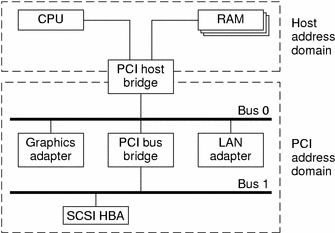
The PCI local bus is a high-performance bus designed for high-speed data transfer. The PCI bus resides on the system board and is normally used as an interconnect mechanism between highly integrated peripheral components, peripheral add-on boards, and host processor or memory systems. The host processor, main memory, and the PCI bus itself are connected through a PCI host bridge, as shown in Figure A-3.
A tree structure of interconnected I/O buses is supported through a series of PCI bus bridges. Subordinate PCI bus bridges can be extended underneath the PCI host bridge to enable a single bus system to be expanded into a complex system with multiple secondary buses. PCI devices can be connected to one or more of these secondary buses. In addition, other bus bridges, such as SCSI or USB, can be connected.
Every PCI device has a unique vendor ID and device ID. Multiple devices of the same kind are further identified by their unique device numbers on the bus where they reside.
Figure A-3 Machine Block Diagram

The PCI host bridge provides an interconnect between the processor and peripheral components. Through the PCI host bridge, the processor can directly access main memory independent of other PCI bus masters. For example, while the CPU is fetching data from the cache controller in the host bridge, other PCI devices can also access the system memory through the host bridge. The advantage of this architecture lies in its separation of the I/O bus from the processor's host bus.
The PCI host bridge also provides data access mappings between the CPU and peripheral I/O devices. It maps every peripheral device to the host address domain so that the processor can access the device through programmed I/O. On the local bus side, the PCI host bridge maps the system memory to the PCI address domain so that the PCI device can access the host memory as a bus master. Figure A-3 shows the two address domains.
PCI Address Domain
The PCI address domain consists of three distinct address spaces: configuration, memory, and I/O space.
PCI Configuration Address Space
Configuration space is defined geographically; in other words, the location of a peripheral device is determined by its physical location within an interconnected tree of PCI bus bridges. A device is located by its bus number and device (slot) number. Each peripheral device contains a set of well-defined configuration registers in its PCI configuration space. The registers are used not only to identify devices but also to supply device configuration information to the configuration framework. For example, base address registers in the device configuration space must be mapped before a device can respond to data access.
The method for generating configuration cycles is host dependent. In IA machines, special I/O ports are used. On other platforms, the PCI configuration space can be memory-mapped to certain address locations corresponding to the PCI host bridge in the host address domain. When a device configuration register is accessed by the processor, the request is routed to the PCI host bridge. The bridge then translates the access into proper configuration cycles on the bus.
PCI Configuration Base Address Registers
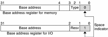
The PCI configuration space consists of up to six 32-bit base address registers for each device. These registers provide both size and data type information. System firmware assigns base addresses in the PCI address domain to these registers.
Each addressable region can be either memory or I/O space. The value contained in bit 0 of the base address register identifies the type. A value of 0 in bit 0 indicates a memory space and a value of 1 indicates an I/O space. Figure A-4 shows two base address registers: one for memory; the other for I/O types.
Figure A-4 Base Address Registers for Memory and I/O

PCI Memory Address Space
PCI supports both 32-bit and 64-bit addresses for memory space. System firmware assigns regions of memory space in the PCI address domain to PCI peripherals. The base address of a region is stored in the base address register of the device's PCI configuration space. The size of each region must be a power of two, and the assigned base address must be aligned on a boundary equal to the size of the region. Device addresses in memory space are memory-mapped into the host address domain so that data access to any device can be performed by the processor's native load or store instructions.
PCI I/O Address Space
PCI supports 32-bit I/O space. I/O space can be accessed differently on different platforms. Processors with special I/O instructions, like the Intel processor family, access the I/O space with in and out instructions. Machines without special I/O instructions will map to the address locations corresponding to the PCI host bridge in the host address domain. When the processor accesses the memory-mapped addresses, an I/O request will be sent to the PCI host bridge, which then translates the addresses into I/O cycles and puts them on the PCI bus. Memory-mapped I/O is performed by the native load/store instructions of the processor.
PCI Hardware Configuration Files
Hardware configuration files should be unnecessary for PCI local bus devices. However, on some occasions drivers for PCI devices need to use hardware configuration files to augment the driver private information. See the driver.conf(4) and pci(4) man pages for further details.
SBus
Typical SBus systems consist of a motherboard (containing the CPU and SBus interface logic), a number of SBus devices on the motherboard itself, and a number of SBus expansion slots. An SBus can also be connected to other types of buses through an appropriate bus bridge.
The SBus is geographically addressed; each SBus slot exists at a fixed physical address in the system. An SBus card has a different address, depending on which slot it is plugged into. Moving an SBus device to a new slot causes the system to treat it as a new device.
The SBus uses polling interrupts. When an SBus device interrupts, the system only knows which of several devices might have issued the interrupt. The system interrupt handler must ask the driver for each device whether it is responsible for the interrupt.
SBus Physical Address Space
Table A-1 shows the physical address space layout of the Sun Ultra 2 computer. A physical address on the Ultra 2 consists of 41 bits. The 41-bit physical address space is further broken down into multiple 33-bit address spaces identified by PA(40:33).
Table A-1 Device Physical Space in the Ultra 2
PA(40:33) | 33-bit Space | Usage |
|---|---|---|
0x0 | 0x000000000 - 0x07FFFFFFF | 2 Gbytes Main memory |
0x80 - 0xDF | Reserved on Ultra 2 | Reserved on Ultra 2 |
0xE0 | Processor 0 | Processor 0 |
0xE1 | Processor 1 | Processor 1 |
0xE2 - 0xFD | Reserved on Ultra 2 | Reserved on Ultra 2 |
0xFE | 0x000000000 - 0x1FFFFFFFF | UPA Slave (FFB) |
0xFF | 0x000000000 - 0x0FFFFFFFF | System I/O space |
| 0x100000000 - 0x10FFFFFFF | SBus Slot 0 |
| 0x110000000 - 0x11FFFFFFF | SBus Slot 1 |
| 0x120000000 - 0x12FFFFFFF | SBus Slot 2 |
| 0x130000000 - 0x13FFFFFFF | SBus Slot 3 |
| 0x1D0000000 - 0x1DFFFFFFF | SBus Slot D |
| 0x1E0000000 - 0x1EFFFFFFF | SBus Slot E |
| 0x1F0000000 - 0x1FFFFFFFF | SBus Slot F |
Physical SBus Addresses
The SBus has 32 address bits, as described in the SBus Specification. Table A-2 describes how the Ultra 2 uses the address bits.
Table A-2 Ultra 2 SBus Address Bits
Bits | Description |
|---|---|
0 - 27 | These bits are the SBus address lines used by an SBus card to address the contents of the card. |
28 - 31 | Used by the CPU to select one of the SBus slots. These bits generate the SlaveSelect lines. |
This addressing scheme yields the Ultra 2 addresses shown in Table A-1. Other implementations might use a different number of address bits.
The Ultra 2 has seven SBus slots, four of which are physical. Slots 0 through 3 are available for SBus cards. Slots 4-12 are reserved. The slots are used in the following way:
Slots 0-3 are physical slots that have DMA-master capability.
Slots D, E, and F are not actual physical slots, but refer to the onboard direct memory access (DMA), SCSI, Ethernet, and audio controllers. For convenience, these are viewed as being plugged into slots D, E, and F.
Note - Some SBus slots are slave-only slots. Drivers that require DMA capability should use ddi_slaveonly(9F) to determine if their device is in a DMA-capable slot. For an example of this function, see "The attach() Entry Point".


