Communication Troubleshooting
Electrical Characteristics
EIA RS-232-C Section 2.3
For data interchange circuits, the signal shall be considered in the marking
condition when the voltage (V1) interchange circuit measured at the
interface point, is more negative than minus three volts with respect to
Circuit AB (Signal Ground). The signal shall be considered in the spacing
condition when the voltage (V1) is more positive than plus three
volts with respect to circuit AB. The signal state in not uniquely defined
when the voltage (V1) is in this transition region.
EIA RS-232-D Section 2.1.3
For data interchange circuits, the signal shall be considered in the marking
condition when the voltage (V1) on the interchange circuit, measured
at the interface point, is more negative than minus three volts with respect
to Circuit AB (Signal Ground). The signal shall be considered in the spacing
condition when the voltage (V1) is more positive than plus three
volts with respect to circuit AB. The region between plus three volts and minus
three volts is defined as the transition region. The signal state in not
uniquely defined when the voltage (V1) is in this transition region.
During the transmission of data, the marking condition shall be used to
denote the binary state ONE and the spacing condition shall be used to denote
state ZERO.
EIA RS-422-A Section 4.1.1
For either binary state, the magnitude of the differential voltage
(V0) measured between the two generator output terminals shall not
be less than 6.0 volts; nor shall the magnitude of V0a and
V0b measured between the two generator output terminals and
generator circuit ground be more than 6.0 volts.
EIA RS-423-A Section 4.1.1
For either binary state, the magnitude of the voltage (V0)
measured between the generator output terminal and generator circuit ground
shall not be less than 4.0 volts nor more than 6.0 volts. For the opposite
binary state, the polarity of V0 shall be reversed.
EIA RS-449-A Section 2.1.1
The following circuits are classified as Category I circuits: SD, RD, TT,
ST, RT, RS, CS, RR, TR, and DM.
For applications where the signaling rate on the data interchange circuits
(Circuits SD and RD) is 20,000 bits per second or less, the individual Category
I circuits shall use either the balanced electrical characteristics of RS-423,
without the cable termination resistance (Rt), or the unbalanced
electrical characteristics of RS-422-A. Two leads shall be brought out to the
interface connector for each Category I circuit. Each interchange circuit
consists of a pair of wires interconnecting a balanced or unbalanced generator
and a differential receiver.
For applications where the signaling rate on the data interchange circuits
(Circuits SD and RD) is above 20,000 bits per second, all Category I circuits
shall use the balanced electrical characteristics of RS-422. Use of optional
cable termination resistance (Rt) permitted. Each interchange
circuit consists of a pair of wires interconnecting a balanced generator and a
differential receiver.
EIA RS-449-A Section 2.1.2
All other circuits are classified as Category II circuits. For all
applications, Category II circuits shall use the unbalanced electrical
characteristics of RS-423. Each Category II interchange circuit consists of one
wire interconnecting an unbalanced generator and a differential receiver.
RS-232 Signals
| PIN |
SIGNAL |
SIGNAL NAME |
FLOW |
DESCRIPTION |
2
14 |
BA
or
TD |
Transmit Data |
Output |
Data transmitted to the data communications equipment. |
3
16 |
BB
or
RD |
Receive Data |
Input |
Data received from the data communications equipment. |
4
19 |
CA
or
RTS |
Request to Send |
Output |
Signal sent to the data communications equipment, asking if it is ready
to start accepting data. |
5
13 |
CB
or
CTS |
Clear to Send |
Input |
Ready to accept data signal from the data communications equipment. |
| 6 |
CC
or
DSR |
Data Set Ready |
Input |
Data communications equipment indicates the status of the local data set. |
| 7 |
AB
or
SG |
Signal Ground |
None |
Signal Ground provides a reference level for the signal voltages. |
8
12 |
CF
or
DCD |
Data Carrier Detect |
Input |
Data communications equipment detected "carrier."
Example: a modem senses tones sent to it by another modem over phone lines. |
| 15 |
DB
or
TC |
Transmit Clock
from DCE |
Input |
Transmit clock from the modem. Usually not used for asynchronous devices
(terminals, printers, and modems, etc.). |
| 17 |
DD
or
RC |
Receive Clock
from DCE |
Input |
Receive clock from the modem. Usually not used for asynchronous devices
(terminals, printers, and modems, etc.). |
| 20 |
CD
or
DTR |
Data Terminal
Ready |
Output |
The DTE is powered on and ready to communicate as the
"local data terminal" with the data communication equipment.
For example, the modem. |
| 24 |
DA
or
TCO |
Transmit Clock
from DTE |
Output |
Provides transmit clock from the DTE. Usually not used for asynchronous
devices (terminals, printers, and modems, etc.). |
RS-449 Signals
| PIN |
SIGNAL |
SIGNAL NAME |
FLOW |
DESCRIPTION |
4
22 |
SD
or
TD |
Transmit Data |
Output |
Data transmitted to the data communications equipment. |
6
24 |
RD |
Receive Data |
Input |
Data received from the data communications equipment. |
7
25 |
RS
or
RTS |
Request to Send |
Output |
Signal sent to the data communications equipment, asking if it is
ready to start accepting data. |
9
27 |
CS
or
CTS |
Clear to Send |
Input |
Ready to accept data signal from the data communications equipment. |
11
29 |
DM
or
DSR |
Data Set Ready |
Input |
Data communications equipment indicates the status of the local data set. |
| 19 |
SG |
Signal Ground |
None |
Signal Ground provides a reference level for the signal voltages. |
13
31 |
RR
or
DCD |
Data Carrier Detect |
Input |
Data communications equipment detected "carrier."
Example: a modem senses tones sent to it by another modem over phone lines. |
5
23 |
ST
or
TC |
Transmit Clock
from DCE |
Input |
Transmit clock from the modem. Usually not used for asynchronous devices
(terminals, printers, and modems, etc.). |
8
26 |
RT
or
RC |
Receive Clock
from DCE |
Input |
Receive clock from the modem. Usually not used for asynchronous devices
(terminals, printers, and modems, etc.). |
12
30 |
TR
or
DTR |
Data Terminal
Ready |
Output |
The DTE is powered on and ready to communicate as the
"local data terminal" with the data communication equipment.
For example, the modem. |
17
35 |
TT
or
TCO |
Transmit Clock
from DTE |
Output |
Provides transmit clock from the DTE. Usually not used for asynchronous
devices (terminals, printers, and modems, etc.). |
Ethernet Controllers
82586
with
8023A |
7990
with
7992 |
7990
with
T7213 |
79C90 |
MACIO
with
T7213 |
MACIO
with
LXT901 |
79C940 |
FEPS |
CHEERIO |
RIO |
Sun-2
3/E
3/110
3/150
3/160
3/180
3200
3400
4100
4400 |
3/50
3/60
3/60LE
4/20
4/25
4/40
4/50
4/60
4/65
4/75
4300
SS10
SS600
SS1000
X450
X453 |
SS10
SS1000
SBE
FSBE
DSBE |
4/50
SS10
FSBE |
4/10
4/15
4/30
SS10SX
SS20 |
SS5
S240
SS4
Xterm 1
A11 |
SQEC |
A12
A14
X1018
X1042
X1049
X1059
X2610
X2611
X2612
X2620
X2622 |
A16
A20/A25
A21/A22
A23
A26
X1032
X1033
X1034
X2630
X2632
CP1500 |
A28
A36 |
MACIO ASIC (NCR 89C100)
The Sun designed MACIO ASIC provides three special purpose SBus DMA channels
commonly used on SPARC platforms: Ethernet, SCSI, and Parallel Port. The
Ethernet block is based on the NCR 92C990 macrocell which is a superset of (and
backward compatible with) the AM7990.
FEPS ASIC (STP2002)
The Sun designed FEPS ASIC is a Fast Ethernet, Parallel Port, and Fast Wide
SCSI controller.
CHEERIO ASIC (STP2003)
The Sun designed CHEERIO ASIC is a Fast Ethernet and 8-Bit
EBus2 controller.
RIO ASIC (SME2300)
The Sun designed RIO ASIC is a Fast Ethernet, IEEE-1394, and
USB controller with an 8-Bit EBus and PCI bridge interface.
Pin Assignments
CPU Serial Ports
RS-232/RS-423
25-Pin Female D-Sub |
| PIN |
SIGNAL |
PIN |
SIGNAL |
| 2 |
TD |
8 |
DCD |
| 3 |
RD |
15 |
TC |
| 4 |
RTS |
17 |
RC |
| 5 |
CTS |
20 |
DTR |
| 6 |
DSR |
24 |
TCO |
| 7 |
GND |
|
|
|
 |
Sun-4/15/30, SS10, SS20, A20,
A25, A26, and A27
Adapter 530-1869 Serial Port A
25-Pin Female D-Sub |
| PIN |
SIGNAL |
PIN |
SIGNAL |
| 2 |
TD |
8 |
DCD |
| 3 |
RD |
15 |
TC |
| 4 |
RTS |
17 |
RC |
| 5 |
CTS |
20 |
DTR |
| 6 |
DSR |
24 |
TCO |
| 7 |
GND |
|
|
|
 |
Sun-4/15/30, SS10, SS20*, A20,
A25, A26, and A27
Adapter 530-1869 Serial Port B
25-Pin Female D-Sub |
| PIN |
SIGNAL |
PIN |
SIGNAL |
| 2 |
TD |
8 |
DCD |
| 3 |
RD |
15 |
TC |
| 4 |
RTS |
20 |
DTR |
| 5 |
CTS |
24 |
TCO |
| 7 |
GND |
|
|
Port B is asynchronous only.
| * |
A jumper setting change and an
adapter cable is required to use the
SS20 Port B in synchronous mode.
Pin-9 is dsr and Pin-10 is rtxc.
|
|
 |
Netra t1 Model 100/105 Serial Port
Netra T1 AC200/DC200 Serial Port
Netra 120 and Sun Fire V120 Serial Port
Netra X1 and Sun Fire V100 Serial Port
Sun Fire V480 Serial Port
RJ45 to DB-25 Serial Adapter 530-2889 |
| RJ45 |
DB25 |
SIGNAL |
|
RJ45 |
DB25 |
SIGNAL |
| 1 |
5 |
RTS |
5 |
7 |
GND |
| 2 |
6 |
DTR |
6 |
2 |
RXD |
| 3 |
3 |
TXD |
7 |
20 |
DSR |
| 4 |
7 |
GND |
8 |
4 |
CTS |
|
 |
JavaStation JJ and JK Serial Port A
Ultra 5 and Ultra 10 Serial Port B
RS-232/RS-423 9-Pin Male D-Sub |
| PIN |
SIGNAL |
PIN |
SIGNAL |
| 1 |
DCD |
5 |
GND |
| 2 |
RD |
6 |
DSR |
| 3 |
TD |
7 |
RTS |
| 4 |
DTR |
8 |
CTS |
| 9 |
RI |
|
|
|
 |
Pin Assignments
CPU Keyboard and Mouse Port
CPU Keyboard and Mouse Port
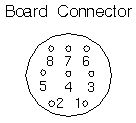
8-Pin Female Mini-Din |
| PIN |
SIGNAL |
PIN |
SIGNAL |
| 1 |
GND |
5 |
TD-KB |
| 2 |
GND |
6 |
RD-KB |
| 3 |
+5Vdc |
7 |
* |
| 4 |
RD-M |
8 |
+5Vdc |
|
 |
| * |
Pin 7 is:
 Connected to Pins 1 and 2 on SS1, SS1+, SS2, IPC, and IPX.
 TD-M on the 4300, 4400, and SS600MP.
 Keyboard Power-On on SS4, SS5, SS10, SS10SX, SS20,
Classic, LX, SS1000, SC2000, A11, A12, A14,
A16, A20, A21, A22, A23, A25, A26, A27, and Ex000.
|
|
JavaStation JJ and JK Mouse Port
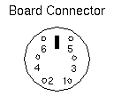
6-Pin Female Mini-Din |
| PIN |
SIGNAL |
PIN |
SIGNAL |
| 1 |
Data |
4 |
+5Vdc |
| 2 |
Reserved |
5 |
Clock |
| 3 |
Ground |
6 |
Reserved |
|
 |
JavaStation JJ and JK Keyboard Port
6-Pin Female Mini-Din |
| PIN |
SIGNAL |
PIN |
SIGNAL |
| 1 |
Data |
4 |
+5Vdc |
| 2 |
Reserved |
5 |
Clock |
| 3 |
Ground |
6 |
Reserved |
|
 |
Pin Assignments
USB Port
|
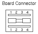
USB Port 4-Pin |
| PIN |
SIGNAL |
PIN |
SIGNAL |
1
2 |
USB0_VCC
CM_USB_D0_N |
3
4 |
CM_USB_D0_P
Ground |
1
2 |
USB1_VCC
CM_USB_D1_N |
3
4 |
CM_USB_D1_P
Ground |
|
 |
Pin Assignments
IEEE-1394 Port
|
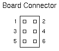
IEEE-1394 Port 6-Pin |
| PIN |
SIGNAL |
PIN |
SIGNAL |
| 1 |
EX_BUSPWR |
2 |
Ground |
| 3 |
TPB1_OUT_N |
4 |
TPB1_OUT_P |
| 5 |
TPA1_OUT_N |
6 |
TPA1_OUT_P |
|
 |
Pin Assignments
CPU Parallel Port
SS5, SS10, and SS20 Parallel Port
Upper 26-Pin Female Hi-Density
SPARCstation Voyager
26-Pin Female Hi-Density |
| PIN |
SIGNAL |
PIN |
SIGNAL |
| 1 |
STROBE |
14 |
AFXT |
| 2 |
DATA 0 |
15 |
ERROR |
| 3 |
DATA 1 |
16 |
RESET |
| 4 |
DATA 2 |
17 |
SLCTIN |
| 5 |
DATA 3 |
18 |
GND |
| 6 |
DATA 4 |
19 |
GND |
| 7 |
DATA 5 |
20 |
GND |
| 8 |
DATA 6 |
21 |
GND |
| 9 |
DATA 7 |
22 |
GND |
| 10 |
ACK |
23 |
GND |
| 11 |
BUSY |
24 |
GND |
| 12 |
PE |
25 |
GND |
| 13 |
SLCTOUT |
26 |
GND |
Use IBM Adapter 530-1861
Use Centronics Adapter 530-1857
|
 |
Parallel Port
Sun-4/15/30, Xterminal 1, SS4, A11, A12, A14,
A16, A20, A21, A22, A23, A25, A26, and A27
25-Pin Female D-Sub |
| PIN |
SIGNAL |
PIN |
SIGNAL |
| 1 |
STROB E |
14 |
AUTOFD |
| 2 |
DATA 0 |
15 |
ERROR |
| 3 |
DATA 1 |
16 |
INIT |
| 4 |
DATA 2 |
17 |
SLCTIN |
| 5 |
DATA 3 |
18 |
GND |
| 6 |
DATA 4 |
19 |
GND |
| 7 |
DATA 5 |
20 |
GND |
| 8 |
DATA 6 |
21 |
GND |
| 9 |
DATA 7 |
22 |
GND |
| 10 |
ACK |
23 |
GND |
| 11 |
BUSY |
24 |
GND |
| 12 |
PE |
25 |
GND |
| 13 |
SLCT |
|
|
|
 |
SS5, SS10, SS20, and SS Voyager
Centronics Parallel Port Adapter 530-1857
26-Pin Hi-Density to 36-Pin Centronics |
| PIN |
SIGNAL |
PIN |
SIGNAL |
| 1 |
STROBE |
15 |
SLCTIN |
| 2 |
DATA 0 |
20 |
GND |
| 3 |
DATA 1 |
21 |
GND |
| 4 |
DATA 2 |
22 |
GND |
| 5 |
DATA 3 |
23 |
GND |
| 6 |
DATA 4 |
24 |
GND |
| 7 |
DATA 5 |
25 |
GND |
| 8 |
DATA 6 |
26 |
GND |
| 9 |
DATA 7 |
27 |
GND |
| 10 |
ACK |
28 |
GND |
| 11 |
BUSY |
31 |
RESET |
| 12 |
PE |
32 |
ERROR |
| 13 |
SLCTOUT |
36 |
SLCTIN |
| 14 |
AFXT |
|
|
|
 |
SS5, SS10, SS20, and SS Voyager
IBM Parallel Port Adapter 530-1861
26-Pin Hi-Density to 25-Pin D-Sub |
| PIN |
SIGNAL |
PIN |
SIGNAL |
| 1 |
STROBE |
14 |
AFXT |
| 2 |
DATA 0 |
15 |
ERROR |
| 3 |
DATA 1 |
16 |
RESET |
| 4 |
DATA 2 |
17 |
SLCTIN |
| 5 |
DATA 3 |
18 |
GND |
| 6 |
DATA 4 |
19 |
GND |
| 7 |
DATA 5 |
20 |
GND |
| 8 |
DATA 6 |
21 |
GND |
| 9 |
DATA 7 |
22 |
GND |
| 10 |
ACK |
23 |
GND |
| 11 |
BUSY |
24 |
GND |
| 12 |
PE |
25 |
GND |
| 13 |
SLCTOUT |
|
|
|
 |
Pin Assignments
AUI Port
SPARCclassic, SS5, and SS20
10BASE-5 Ethernet AUI Port
Lower 26-Pin Female Hi-Density |
| PIN |
SIGNAL |
PIN |
SIGNAL |
| 1 |
E.TD- |
14 |
E.TD+ |
| 2 |
E.RD+ |
15 |
E.RD- |
| 3 |
E.COL- |
16 |
E.COL+ |
| 4 |
E.+12Vdc |
17 |
E.GND |
| 5 |
Unused |
18 |
Unused |
| 6 |
Unused |
19 |
Unused |
| 7 |
Unused |
20 |
Unused |
| 8 |
Unused |
21 |
Unused |
| 9 |
Unused |
22 |
Unused |
| 10 |
Unused |
23 |
Unused |
| 11 |
Unused |
24 |
Unused |
| 12 |
Unused |
25 |
Unused |
| 13 |
Unused |
26 |
Unused |
Use AUI Adapter 530-2021
|
 |
Pin Assignments
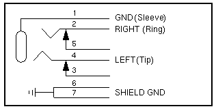
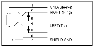
Sun Microphone II
| Sun Microphone II |

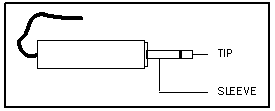
The Microphone II is not compatible with Sun4c systems. |
SS5 / SS4 Audio Module
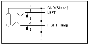
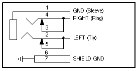
SS5 and SS4 Audio Module 501-2592 Line-In Jack
 |
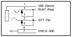
SS5 and SS4 Audio Module 501-2592 Line-Out Jack
 |
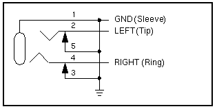
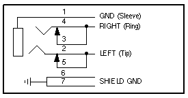
SS5 and SS4 Audio Module 501-2592 Microphone Jack
 |
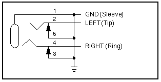
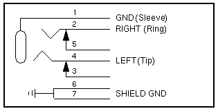
SS5 and SS4 Audio Module 501-2592 Headphone Jack
 |
SS20 Audio Jacks
SS20 Line-In Jack
 |
SS20 Line-Out Jack
 |
SS20 Microphone Jack
 |
SS20 Headphone Jack
 |
A11 / A12 / A14 Audio Jacks
A11, A12, and A14 Line-In Jack
 |
A11, A12, and A14 Line-Out Jack
 |
A11, A12, and A14 Microphone Jack
 |
A11, A12, and A14 Headphone Jack
 |
10BASE-5 / 10BASE-T Ethernet
10BASE-5 Ethernet
8-Pin Female Mini-Din |
| PIN |
SIGNAL |
PIN |
SIGNAL |
| 2 |
COL+ |
9 |
COL- |
| 3 |
TD+ |
10 |
TD- |
| 5 |
RD+ |
12 |
RD- |
| 6 |
GND |
13 |
+12Vdc |
|
 |
10BASE-T Ethernet
8-Pin RJ45 |
| PIN |
SIGNAL |
PIN |
SIGNAL |
| 1 |
TPO+ |
5 |
Unused |
| 2 |
TPO- |
6 |
TPI- |
| 3 |
TPI+ |
7 |
Unused |
| 4 |
Unused |
8 |
Unused |
|
 |
Sunlink ISDN
| SunLink IDSN |
| SUPPORTED SunLink ISDN CARRIERS |
SPECIFICATION |
| British Telecom |
ISDN2 |
| Deutsche Bundepost Telekom |
1TR6 |
| France Telecom Numeris |
VN2 |
| Nippon Telegraph and Telephone |
INS-Net 64 |
| AT&T 5ESS 5e5 conformant US carriers |
AT&T 5ESS 5e5 |
|
ISDN Network Termination NT
8-Pin RJ45 |
| PIN |
SIGNAL |
PIN |
SIGNAL |
| 1 |
PS3+ |
5 |
TD- |
| 2 |
PS3- |
6 |
RD- |
| 3 |
RD+ |
7 |
PS2- |
| 4 |
TD+ |
8 |
PS2+ |
|
 |
ISDN Terminal Endpoint TE
8-Pin RJ45 |
| PIN |
SIGNAL |
PIN |
SIGNAL |
| 1 |
PS3+ |
5 |
RD-- |
| 2 |
PS3- |
6 |
TD-- |
| 3 |
TD+ |
7 |
PS2- |
| 4 |
RD+ |
8 |
PS2+ |
|
 |
SBE/S 10BASE-5 and 10BASE-T Ethernet
SBE/S 10BASE-T and 10BASE-5
14-Pin Champ |
| PIN |
SIGNAL |
PIN |
SIGNAL |
| 1 |
COL+ |
8 |
COL- |
| 2 |
TD+ |
9 |
TD- |
| 3 |
RD+ |
10 |
RD- |
| 4 |
GND |
11 |
+12Vdc |
| 5 |
GND |
12 |
+12Vdc |
| 6 |
TPO+ |
13 |
TPO- |
| 7 |
TPI+ |
14 |
TPI- |
|
 |
SBE/S 10BASE-5 Adapter 530-1812
15-Pin Female D-Sub |
| PIN |
SIGNAL |
PIN |
SIGNAL |
| 1 |
GND |
9 |
COL- |
| 2 |
COL+ |
10 |
TD- |
| 3 |
TD+ |
11 |
GND |
| 4 |
GND |
12 |
RD- |
| 5 |
RD+ |
13 |
+12Vdc |
| 6 |
GND |
14 |
GND |
| 7 |
Unused |
15 |
Unused |
| 8 |
GND |
|
|
|
 |
SBE/S 10BASE-T Adapter 530-1813
8-Pin RJ45 |
| PIN |
SIGNAL |
PIN |
SIGNAL |
| 1 |
TPO+ |
5 |
Unused |
| 2 |
TPO- |
6 |
TPI- |
| 3 |
TPI+ |
7 |
Unused |
| 4 |
Unused |
8 |
Unused |
|
 |
Fast Ethernet
Fast Ethernet 10BASE-T/100BASE-T Port
8-Pin RJ45 |
| PIN |
SIGNAL |
PIN |
SIGNAL |
| 1 |
TX+ |
5 |
Unused |
| 2 |
TX- |
6 |
RX- |
| 3 |
RX+ |
7 |
Unused |
| 4 |
Unused |
8 |
Unused |
|
 |
Fast Ethernet MII Port
40-Pin Female Hi-Density |
| PIN |
SIGNAL |
PIN |
SIGNAL |
| 1 |
PWR |
21 |
PWR |
| 2 |
MDIO |
22 |
GND |
| 3 |
MDC |
23 |
GND |
| 4 |
RXD3 |
24 |
GND |
| 5 |
RXD2 |
25 |
GND |
| 6 |
RXD1 |
26 |
GND |
| 7 |
RXD0 |
27 |
GND |
| 8 |
RXDV |
28 |
GND |
| 9 |
RXCLK |
29 |
GND |
| 10 |
RXER |
30 |
GND |
| 11 |
TXER |
31 |
GND |
| 12 |
TXCLK |
32 |
GND |
| 13 |
TXEN |
33 |
GND |
| 14 |
TXD0 |
34 |
GND |
| 15 |
TXD1 |
35 |
GND |
| 16 |
TXD2 |
36 |
GND |
| 17 |
TXD3 |
37 |
GND |
| 18 |
COL |
38 |
GND |
| 19 |
CRS |
39 |
GND |
| 20 |
PWR |
40 |
PWR |
|
 |
SPARCcluster PDB Ethernet Cable 530-2149 and 530-2150
8-Pin RJ45
 |
SPC/S
SPC/S RS-232/RS423 Serial Ports
25-Pin Female D-Sub |
| PIN |
SIGNAL |
PIN |
SIGNAL |
| 2 |
TD |
6 |
DSR |
| 3 |
RD |
7 |
GND |
| 4 |
RTS |
8 |
DCD |
| 5 |
CTS |
20 |
DTR |
|
 |
SPC/S Parallel Port
25-Pin Female D-Sub |
| PIN |
SIGNAL |
PIN |
SIGNAL |
| 1 |
STROBE |
14 |
AFXN |
| 2 |
DATA 0 |
15 |
ERROR |
| 3 |
DATA 1 |
16 |
RESET |
| 4 |
DATA 2 |
17 |
SLCI_IN |
| 5 |
DATA 3 |
18 |
GND |
| 6 |
DATA 4 |
19 |
GND |
| 7 |
DATA 5 |
20 |
GND |
| 8 |
DATA 6 |
21 |
GND |
| 9 |
DATA 7 |
22 |
GND |
| 10 |
ACK |
23 |
GND |
| 11 |
BUSY |
24 |
GND |
| 12 |
PE |
25 |
GND |
| 13 |
SLCT_OU T |
|
|
|
 |
HSI/S
HSI/S RS-449 Ports 0, 1, 2, and 3
37-Pin Female D-Sub |
| PIN |
SIGNAL |
PIN |
SIGNAL |
| 4 |
SD- |
22 |
SD+ |
| 5 |
ST- |
23 |
ST+ |
| 6 |
RD- |
24 |
RD+ |
| 7 |
RS- |
25 |
RS+ |
| 8 |
RT- |
26 |
RT+ |
| 9 |
CS- |
27 |
CS+ |
| 11 |
DM- |
29 |
DM+ |
| 12 |
TR- |
30 |
TR+ |
| 13 |
RR- |
31 |
RR+ |
| 17 |
TT- |
35 |
TT+ |
| 19 |
GND |
|
|
|
 |
Remote System Control (RSC)
RSC Serial Connector
8-Pin RJ45 |
| RJ45 |
SIGNAL |
|
RJ45 |
SIGNAL |
| 1 |
RTS |
5 |
GND |
| 2 |
DTR |
6 |
RXD |
| 3 |
TXD |
7 |
DSR |
| 4 |
GND |
8 |
CTS |
|
 |
RSC Modem Connector
4-Pin RJ11 |
| RJ11 |
SIGNAL |
|
RJ11 |
SIGNAL |
| 1 |
No connection |
3 |
Tip |
| 2 |
Ring |
4 |
No connection |
|
 |
RSC Ethernet Connector
8-Pin RJ45 |
| RJ45 |
SIGNAL |
|
RJ45 |
SIGNAL |
| 1 |
TXD/RXD 0 + |
5 |
TXD/RXD 2 - |
| 2 |
TXD/RXD 0 - |
6 |
TXD/RXD 1 - |
| 3 |
TXD/RXD 1 + |
7 |
TXD/RXD 3 + |
| 4 |
TXD/RXD 2 + |
8 |
TXD/RXD 3 - |
|
 |
|


